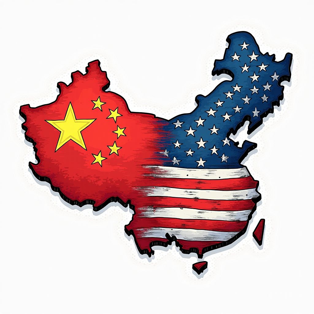
How China's Rare Earth Monopoly is Reshaping the Global AI Industry
Beijing, Tuesday, 10 March 2026.
Controlling 90% of processed rare earths, China is strategically reshaping global AI hardware supply chains in 2026, exposing critical vulnerabilities for United States technology firms.