Applied Materials Enhances Chip Inspection with Advanced eBeam System
Santa Clara, Wednesday, 19 February 2025.
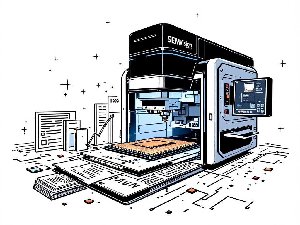
Applied Materials has launched the SEMVision™ H20 to improve semiconductor defect review, using AI and advanced imaging for faster results, potentially transforming chip manufacturing processes.
Breakthrough in Semiconductor Inspection
Applied Materials (NYSE: AMAT) unveiled its latest innovation, the SEMVision™ H20 defect review system, on February 19, 2025 [1]. This next-generation system integrates advanced AI image recognition with enhanced eBeam technology to detect nanoscale defects in semiconductor manufacturing [1]. The system’s pioneering second-generation ‘cold field emission’ technology enables sub-nanometer accuracy in defect detection, marking a significant advancement in chip inspection capabilities [1].
Performance Improvements and Industry Impact
The SEMVision H20 delivers remarkable efficiency gains, processing results up to three times faster than existing advanced techniques [1]. Keith Wells, Group Vice President of Imaging and Process Control at Applied Materials, emphasizes that the system helps chipmakers better manage the massive amounts of data from inspection tools [1]. This advancement is particularly crucial as traditional optical inspection techniques struggle to handle the 100 times increase in defect candidates at advanced nodes [1].
Technology Leadership and Market Position
Applied Materials maintains its position as a leader in materials engineering solutions, enabling the production of virtually every new chip and advanced display globally [2]. The company’s expertise in atomic-level materials modification has been recognized industry-wide, with Applied Materials ranking highest among Wafer Fab Equipment companies on the Intellectual Property Owners Association’s list of top U.S. patent recipients [2]. The launch of SEMVision H20 strengthens the company’s eBeam product family, which is already the most widely used review system in the world [1].
Future Implications and Industry Events
The timing of this launch aligns with the upcoming SPIE Advanced Lithography and Patterning Conference (February 23-27, 2025, in San Jose, California) [5], where industry leaders will discuss advanced semiconductor manufacturing technologies. The SEMVision H20 system is positioned to play a crucial role in upcoming manufacturing processes for 2nm node chips and advanced memory technologies [1], addressing the semiconductor industry’s growing demands for more precise and efficient inspection solutions.