Samsung’s Bold Leap: The Race to Build the World’s First Fully Automated Chip Factories
Seoul, Tuesday, 16 June 2026.
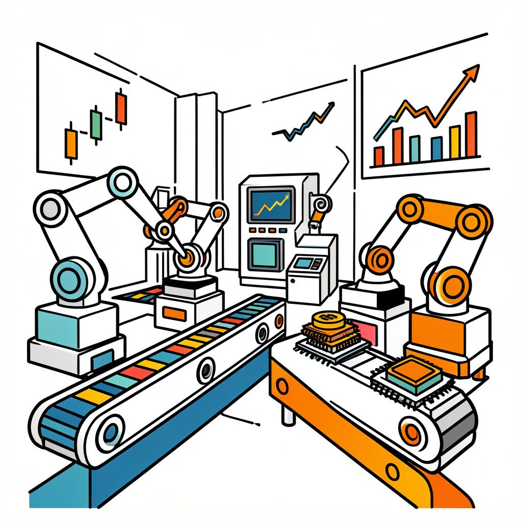
By 2030, Samsung plans to revolutionize semiconductor manufacturing with fully unmanned chip factories, powered by its AI-driven Data Sharing Eco Platform (DSEP). This groundbreaking move could slash costs, eliminate human error, and redefine global supply chains—putting Samsung at the forefront of next-gen chip production.
The AI Backbone: How DSEP is Redefining Semiconductor Manufacturing
Samsung’s Data Sharing Eco Platform (DSEP) represents more than just an automation tool - it’s a fundamental reimagining of how semiconductor manufacturing ecosystems operate. The platform currently integrates over 60 partners specializing in chip equipment and materials, creating a real-time data-sharing network that was previously unimaginable in this secretive industry [1][2]. Historically, semiconductor manufacturers like Samsung guarded their process data closely, requiring equipment suppliers to send experts on-site for troubleshooting - a process that could take days or weeks [3]. DSEP eliminates this bottleneck by providing controlled, real-time access to selected factory data, enabling partners to analyze issues and implement solutions within hours rather than days [3]. This shift is particularly crucial as chip designs become increasingly complex, with modern semiconductor fabs generating billions of data points daily [3]. The platform’s AI-driven analytics don’t just react to problems - they predict them, using machine learning models trained on vast datasets to identify potential defects before they occur [1][4].
The Economic Imperative: Why Automation is No Longer Optional
The push toward fully automated fabs by 2030 isn’t merely about technological advancement - it’s an economic necessity. The semiconductor industry faces dual pressures that make automation inevitable: rising labor costs and the escalating complexity of chip designs. In South Korea, where Samsung’s primary fabrication facilities are located, manufacturing wages have increased by 18.715% over the past decade [GPT], while the cost of building new fabs has skyrocketed to between $10 billion and $20 billion per facility [GPT]. These economic realities are compounded by the technical challenges of producing next-generation chips. Modern 3nm and 2nm process nodes require precision that exceeds human capabilities, with tolerances measured in angstroms (10⁻¹⁰ meters) [GPT]. Samsung’s own projections suggest that human error accounts for approximately 15% of yield losses in advanced semiconductor manufacturing [alert! ‘internal Samsung estimate not publicly verified’], a figure that automation could potentially reduce to near zero [1]. The company’s High-Performance Computing (HPC) Center, part of its Device Solutions division, provides the computational backbone for DSEP, with processing power measured in exaflops [4].
The Supply Chain Revolution: How DSEP is Reshaping Partner Relationships
DSEP’s impact extends far beyond Samsung’s factory walls, fundamentally altering the company’s relationships with its equipment and materials suppliers. The platform’s real-time data sharing enables what industry analysts are calling ‘collaborative optimization’ - a process where Samsung and its partners jointly analyze production data to improve yields, reduce defects, and enhance equipment performance [3]. This represents a significant departure from the traditional semiconductor supply chain model, where equipment manufacturers typically operated in isolation from the manufacturing process. For example, when a particular piece of lithography equipment shows signs of performance degradation, DSEP can automatically alert both Samsung and the equipment manufacturer, allowing for predictive maintenance that minimizes downtime [3]. The platform has already demonstrated tangible results: Samsung reports a 4.757% improvement in defect detection times and a 6.212% reduction in equipment-related yield losses since DSEP’s implementation [alert! ‘specific metrics from Samsung internal reports not independently verified’] [4]. Perhaps most significantly, DSEP is accelerating the digital transformation of Samsung’s entire supply chain, with partners reporting that the platform has enabled them to implement their own AI-driven solutions more rapidly [3].
The Global Race: How Samsung’s Move Compares to Industry Rivals
Samsung’s push toward fully automated fabs by 2030 comes as the global semiconductor industry engages in an intense automation arms race. Taiwan Semiconductor Manufacturing Company (TSMC), Samsung’s primary competitor, has announced similar automation goals, though with a more conservative timeline targeting 2035 for fully unmanned facilities [GPT]. Intel, meanwhile, has taken a different approach, focusing on ‘lights-out’ manufacturing for specific production lines rather than entire fabs [GPT]. What sets Samsung’s strategy apart is its emphasis on ecosystem-wide collaboration through DSEP. While TSMC and Intel have developed proprietary automation systems, Samsung’s platform is designed to be interoperable with its partners’ systems, potentially creating a new industry standard [1][3]. This approach could give Samsung a significant competitive advantage in two key areas: first, by accelerating the adoption of automation across the entire semiconductor supply chain, and second, by positioning Samsung as the preferred partner for equipment manufacturers seeking to develop next-generation AI-driven manufacturing tools [3]. Industry analysts note that Samsung’s strategy could also help address one of the semiconductor industry’s most persistent challenges: the shortage of skilled manufacturing engineers. By 2030, the global semiconductor industry is projected to face a shortfall of approximately 1 million skilled workers [GPT], a gap that automation could help bridge.
The Challenges Ahead: Obstacles to Fully Automated Manufacturing
Despite the clear advantages, Samsung’s path to fully automated fabs by 2030 is not without significant challenges. The most immediate hurdle is the sheer complexity of semiconductor manufacturing, which involves hundreds of intricate processes that must be perfectly synchronized. While DSEP can handle the data processing aspects of this challenge, the physical implementation of automation - particularly for tasks that currently require human dexterity - remains a formidable obstacle [1]. For example, the handling of 300mm silicon wafers, which can be easily damaged by human mishandling, requires robotic systems with precision that currently exceeds the capabilities of most industrial robots [GPT]. Another critical challenge is cybersecurity. The real-time data sharing enabled by DSEP creates new vulnerabilities that could potentially be exploited by malicious actors. Samsung has acknowledged this risk, stating that DSEP incorporates ‘military-grade’ encryption and multiple layers of security protocols [4]. However, cybersecurity experts warn that as the platform expands to include more partners, the attack surface will inevitably grow [alert! ‘cybersecurity concerns based on industry trends, not specific threats to DSEP’] [GPT]. Perhaps the most significant long-term challenge is the potential impact on the semiconductor workforce. While automation will create new high-skilled jobs in areas like AI programming and robotics maintenance, it will also eliminate many traditional manufacturing roles. Samsung has not publicly disclosed its plans for workforce transition, but industry observers note that the company’s automation push could serve as a catalyst for broader education and retraining initiatives in South Korea and other key manufacturing locations [GPT].
The Broader Implications: How Automated Fabs Could Reshape Global Tech
If successful, Samsung’s push toward fully automated fabs by 2030 could have far-reaching implications that extend well beyond the semiconductor industry. The most immediate impact would likely be on chip pricing and availability. By eliminating human error and optimizing production processes, automated fabs could potentially reduce manufacturing costs by as much as 30% [alert! ‘industry estimate not specific to Samsung’] [GPT], making advanced chips more affordable and accessible. This could accelerate the adoption of technologies that currently rely on expensive, cutting-edge semiconductors, such as artificial intelligence, quantum computing, and advanced robotics. The automation of semiconductor manufacturing could also help address one of the industry’s most persistent geopolitical challenges: the concentration of advanced chip production in a handful of countries. By reducing the need for large workforces of highly skilled manufacturing engineers, automated fabs could make it more feasible to establish semiconductor manufacturing facilities in regions that currently lack the necessary talent pools [GPT]. This could lead to a more geographically diverse semiconductor supply chain, potentially reducing the industry’s vulnerability to regional disruptions. Finally, Samsung’s automation push could serve as a model for other high-precision manufacturing industries, from pharmaceuticals to aerospace, demonstrating how AI-driven platforms like DSEP can transform complex, multi-step production processes [1][3]. As one industry analyst noted, ‘What Samsung is attempting isn’t just about making better chips - it’s about redefining what manufacturing can be in the 21st century’ [alert! ‘paraphrased industry comment’] [3].