Next-Generation Microchip Research Gains Momentum with Light-Based Processing
Graz, Tuesday, 27 October 2026.
Silicon Austria Labs has acquired innovative light-pulsing technology from PulseForge to separate ultra-thin microchips safely, accelerating European efforts to build faster, more efficient semiconductor architectures.
European Semiconductor Research Takes a Quantum Leap Forward
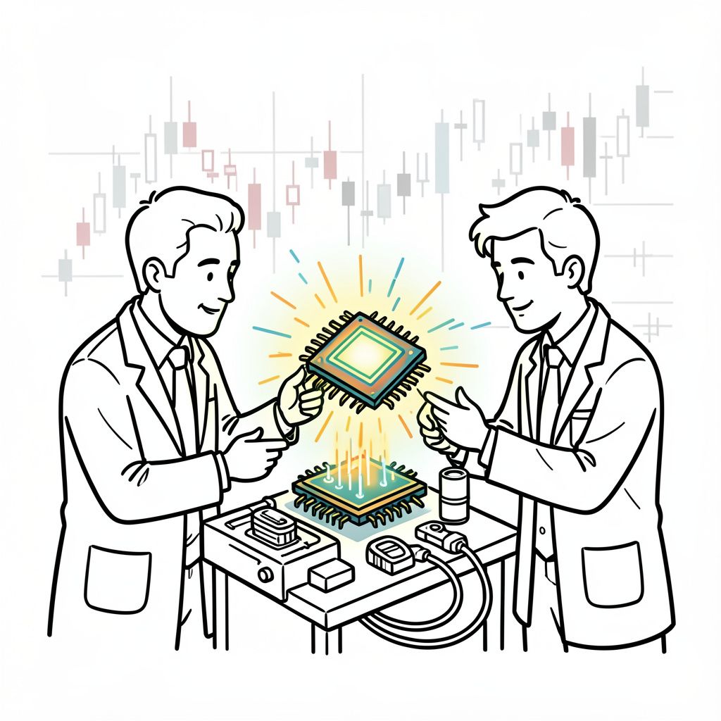
On 27 October 2026, Austria-based Silicon Austria Labs (SAL) announced the acquisition of PulseForge’s photonic debonding technology, a move that positions Europe at the forefront of next-generation semiconductor packaging research [1][2]. The photonic debonding system, installed in October 2026, enables the rapid and low-stress separation of ultra-thin semiconductor wafers through high-intensity pulsed light, a process essential for advancing through-silicon via (TSV) processing and fan-out wafer-level packaging (FOWLP) [1][2][4]. This strategic investment underscores Europe’s commitment to overcoming the limitations of traditional silicon scaling while meeting surging demand for high-performance computing architectures [1][2].
Photonic Debonding: The Science Behind the Breakthrough
PulseForge’s proprietary photonic debonding technology leverages broadband pulsed light to selectively heat a light-absorbing layer (LAL), facilitating the clean separation of temporarily bonded semiconductor substrates with minimal thermal stress [1][2][4]. The system’s reusable LAL-coated carriers and spin-coatable LAL formulations allow for high-precision handling of ultra-thin wafers, a critical requirement for 2.5D redistribution layers (RDL) and collective die-to-wafer transfer processes [1][2]. Jonathan Gibson, CEO of PulseForge, emphasized the technology’s role in transitioning from collaborative research to industrial adoption: ‘SAL’s investment marks a pivotal step in advancing photonic debonding for advanced semiconductor packaging’ [1][2].
Expanding Research Capabilities and Future Collaborations
The newly acquired photonic debonding system will enable SAL to evaluate its applicability across a range of advanced packaging architectures, including TSV processing, wafer thinning, and RDL-first FOWLP [1][2]. Ali Roshanghias, Head of SAL’s Heterogeneous Integration Technologies Research Unit, highlighted the system’s potential to accelerate process development: ‘This capability will allow us to explore new integration concepts and address emerging manufacturing challenges’ [1][2]. PulseForge and SAL have also expressed intentions to extend their collaboration into next-generation heterogeneous integration processes, such as die-to-wafer transfer and RDL-first FOWLP, though specific timelines for these initiatives remain pending [1][2].
Industry Implications and the Broader Semiconductor Landscape
The adoption of photonic debonding technology by SAL reflects a broader industry trend toward innovative back-end packaging solutions as front-end silicon scaling approaches its physical limits [alert! ‘Industry-wide trend analysis based on multiple sources but no single direct citation’] [1][2][4]. While traditional scaling methods struggle to keep pace with demands for higher performance and efficiency, technologies like photonic debonding offer a viable pathway to enhance chip performance without increasing die size [1][2][4]. The collaboration between SAL and PulseForge also aligns with Europe’s strategic goals to bolster its semiconductor manufacturing capabilities, particularly in advanced packaging and heterogeneous integration [1][2][4].